Latest Power Electronics MCQs – New Power Electronics Devices MCQs ( Power Electronics ) MCQs

Latest Power Electronics MCQs
By practicing these MCQs of Power Electronics Devices MCQs ( Power Electronics ) MCQs – Latest Competitive MCQs , an individual for exams performs better than before. This post comprising of objective questions and answers related to “ Power Electronics Devices MCQs ( Power Electronics ) Mcqs “. As wise people believe “Perfect Practice make a Man Perfect”. It is therefore practice these mcqs of Power Electronics to approach the success. Tab this page to check ” Power Electronics Devices MCQs ( Power Electronics )” for the preparation of competitive mcqs, FPSC mcqs, PPSC mcqs, SPSC mcqs, KPPSC mcqs, AJKPSC mcqs, BPSC mcqs, NTS mcqs, PTS mcqs, OTS mcqs, Atomic Energy mcqs, Pak Army mcqs, Pak Navy mcqs, CTS mcqs, ETEA mcqs and others.
Power Electronics MCQs – Power Electronics Devices MCQs ( Power Electronics ) MCQs
The most occurred mcqs of Power Electronics Devices MCQs ( Power Electronics ) in past papers. Past papers of Power Electronics Devices MCQs ( Power Electronics ) Mcqs. Past papers of Power Electronics Devices MCQs ( Power Electronics ) Mcqs . Mcqs are the necessary part of any competitive / job related exams. The Mcqs having specific numbers in any written test. It is therefore everyone have to learn / remember the related Power Electronics Devices MCQs ( Power Electronics ) Mcqs. The Important series of Power Electronics Devices MCQs ( Power Electronics ) Mcqs are given below:
Thyristors-3
1. During the transition time or turn-on time
a) The forward anode voltage decreases from 90 % to 10 % & the anode current also decreases from 90 to 10 % of the initial value
b) The forward anode voltage increases from 10 % to 90 % & the anode current also increases from 10 % to 90 % of the initial value
c) The forward anode voltage decreases from 90 % to 10 % & the anode current increases from 10 % to 90 % of the initial value
d) The forward anode voltage increases from 10 % to 90 % & the anode current decreases from 90% to 10% of the initial value
Answer: c
Explanation: During the turn on time, the voltage across the SCR is going down and the current through it is slowly rising as it is going into the conduction mode.
2. For an SCR the total turn-on time consists of
i) Delay time
ii) Rise time and
iii) Spread time
During the delay time the
a) anode current flows only near the gate
b) anode current rises from zero to very high value
c) losses are maximum
d) anode to cathode voltage is zero
Answer: a
Explanation: Initially for a fraction of a microsecond (delay time) after the gate signal is applied the anode current only flows near the gate terminal where the gate current density is maximum, as the gate current takes some time to spread all over the cross section of the device.
3. The minimum value of anode current below which it must fall to completely turn-off the device is called as the
a) holding current value
b) latching current value
c) switching current value
d) peak anode current value
Answer: a
Explanation: The device will remain in the conducting state unless the anode current falls below the holding current value.
4. For an SCR the total turn-on time consists of
i) Delay time
ii) Rise time and
iii) Spread time
During the rise time the
a) anode current flows only near the gate
b) anode current rises from zero to very high value
c) losses are maximum
d) anode to cathode voltage is zero
Answer: c
Explanation: The losses are maximum during the rise time because both Ia & Va are high.
5. The latching current is _________ than the holding current
a) lower
b) higher
c) same as
d) negative of
Answer: b
Explanation: The latching current is the value of current on which the device will remain in the on state even after removal of the gate signal. Whereas, the holding current is the threshold above which the device will work.
6. For an SCR the total turn-on time consists of
i) Delay time
ii) Rise time and the
iii) Spread time
The spread time interval depends upon
a) the value of gate current
b) junction temperature
c) area of the cathode
d) area of the anode
Answer: c
Explanation: During the spread time the conduction starts spreading all over the SCR cathode cross-section structure, which depends upon the structure of the gate & cathode. Higher the cathode area more is the time required for the charges to spread all over.
7. For effective turning off of the SCR after the anode current has reached zero value, ______________
a) chargers are injected by applying reverse anode-cathode voltage
b) chargers are removed by applying reverse anode-cathode voltage
c) chargers are injected by applying gate signal
d) chargers are removed by applying gate signal
Answer: b
Explanation: To enable the device to regain its reverse blocking capabilities, the stored charges in the junctions of the SCR must be removed.
8. To avoid commutation failure
a) circuit turn-off time must be greater than the thyristor turn-off time
b) circuit turn-off time must be lesser than the thyristor turn-off time
c) circuit turn-off time must be equal to the thyristor turn-off time
d) none of the above mentioned
Answer: a
Explanation: If the thyristor turn off time is more than the circuit turn off time, the circuit will be turned off and the thyristor will keep conducting, which is not at all desirable.
9. The gate characteristics of thyristor is a plot of
a) Vg on the X-axis & Ig on the Y-axis
b) Ig on the X-axis & Vg on the Y-axis
c) Va on the X-axis & Ig on the Y-axis
d) Ig on the X-axis & Va on the Y-axis
Answer: b
Explanation: It is the gate current versus the gate voltage plot and gives the minimum and maximum values of gate parameters.
10. The area under the curve of the gate characteristics of thyristor gives the
a) total average gate current
b) total average gate voltage
c) total average gate impedance
d) total average gate power dissipation
Answer: d
Explanation: As the gate characteristics is a plot of Ig vs Vg consisting of two curves one for the maximum values & other for the minimum the area between them gives the total average gate power dissipation. (A very important parameter in designing of the triggering circuits).
Thyristors-4
1. A tangent drawn from the Y-axis to the Pavg on the gate characteristics gives the value of the
a) maximum value of gate-source resistance
b) minimum value of gate-source resistance
c) maximum value of gate-source power
d) minimum value of gate-source power
Answer: b
Explanation: It gives the min gate to source resistance.
2. Higher the magnitude of the gate pulse
a) lesser is the time required to inject the charges
b) greater is the time required to inject the charges
c) greater is the value of anode current
d) lesser is the value of anode current
Answer: a
Explanation: Lesser time is required to inject the charges & turn on the device with higher gate pulse magnitude.
3.The average gate power dissipation for an SCR is 0.5 Watts the voltage applied to the gate is Vg = 10 V. What is the maximum value of current Ig for safe operation?
a) 0.25 A
b) 10 A
c) 0.05 A
d) 0.1 A
Answer: c
Explanation: Vg.Ig = 0.5 W, the power dissipation mustn’t exceed the average power dissipation.
4. For an SCR, the gate-cathode characteristic has a slop of 130. The gate power dissipation is 0.5 watts. Find Ig
a) 0.62 A
b) 620 mA
c) 62 mA
d) 6.2 mA
Answer: c
Explanation: Vg/Ig = 130 .. (given)
Vg.Ig = 0.5 watts .. (given)
use both the given data & find the gate current.
5. The two transistor model of the SCR can obtained by
a) bisecting the SCR vertically
b) bisecting the SCR horizontally
c) bisecting the SCRs top two & bottom two layers
d) bisecting the SCRs middle two layers
Answer: d
Explanation: The two transistor model consists of p-n-p and n-p-n transistors, of which the middle n-p layer is common in both the transistors.
6. Latching current for an SCR is 100 mA, DC source of 200 V is also connected from the SCR to the L load. Compute the minimum width of the gate pulse required to turn on the device. Take L = 0.2 H.
a) 50 μsec
b) 100 μsec
c) 150 μsec
d) 200 μsec
Answer: b
Explanation: For L load, E = L di/dt
I = E/L t
Therefore, 0.100 = 200t/0.2
T = 100 μsec.
7. The gate-source voltage is Es = 16 V and the load line has a slope of 128 V/A. Calculate the gate current for an average gate power dissipation of 0.5 W.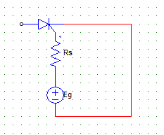
a) 62.5 mA
b) 100.25 mA
c) 56.4 mA
d) 80.65 mA
Answer: a
Explanation: Load line is nothing but Rs
Es = 16V
Vg.Ig = 0.5
Rs = 128
We have Es = Ig x Rs + Vg.
8. From the two transistor (T1 & T2) analogy of SCR, the total anode current of SCR is ___________ in the equivalent circuit.
a) the sum of both the base currents
b) the sum of both the collector current
c) the sum of base current of T1 & collector current of T2
d) the sum of base current of T2 & collector current of T1
Answer: b
Explanation: The sum of both the collector currents of T1 and T2 forms the total anode current of SCR. Refer the model.
9. Consider the two transistor analogy of SCR, if α1 & if α2 are the common-base current gains of both the transistors then to turn-on the device
a) α1 + α2 should approach zero
b) α1 x α2 should approach unity
c) α1 – α2 should approach zero
d) α1 + α2 should approach unity
Answer: d
Explanation: To turn on the device sum of both the current gains should approach unity value.
10. Latching current for an SCR is 100 mA, a dc source of 200 V is also connected to the SCR which is supplying an R-L load. Compute the minimum width of the gate pulse required to turn on the device. Take L = 0.2 H & R = 20 ohm both in series.
a) 62.7 μsec
b) 100.5 μsec
c) 56.9 μsec
d) 81 μsec
Answer: b
Explanation;
E = Ri + L di/dt
Solve the above D.E for I & substitute the above values.
t = 100.503 μsec.
Thyristor Ratings
1. The voltage safety factor (VSF) for an SCR is the ratio of
a) peak working voltage & peak reverse repetitive voltage
b) dv/dt & di/dt
c) peak repetitive reverse voltage & maximum value of input voltage
d) peak repetitive reverse voltage & rms value of input voltage
Answer: c
Explanation: It is peak repetitive reverse voltage/ the maximum value of input voltage(Vm).
2. The forward dv/dt rating of an SCR
a) increases with increase in the junction temperature
b) decreases with increase in the junction temperature
c) increases with decrease in the rms value of forward anode-cathode voltage
d) decreases with decrease in the rms value of forward anode-cathode voltage
Answer: a
Explanation: If the temperature is high, lesser dv/dt is required to turn on the device as the higher temperature has already excited few of the holes & electrons.
3. The finger voltage of an SCR is
a) minimum value of Vak to turn on the device with gate triggering
b) maximum value of Vak to turn on the device with gate triggering
c) minimum value of Vak to turn on the device without gate triggering
d) maximum value of Vak to turn on the device without gate triggering
Answer: a
Explanation: Finger voltage is the minimum value of Vak (anode to cathode voltage) to turn on the device with gate triggering, it is to be avoided for accidental turn-on of the device.
4. Which among the following anode current waveforms will have the minimum junction temperature?
a) 100 % DC
b) 25 % DC
c) 50 % DC
d) AC
Answer: b
Explanation: N % DC is nothing but a wave with n % duty cycle. Lower the Duty cycle lesser is the current flowing & lesser is the temperature dissipation.
5. An SCR has half cycle surge current rating of 3000 A for 50 Hz. Calculate its one-cycle surge current rating
a) 3121.32 A
b) 2121.32 A
c) 3131.32 A
d) 2131.32 A
Answer: b
Explanation: By equating the energies involved in one cycle & subcycle
I2.T = Isb2.t
Isb = 3000 A
T = 1/50
t = T/2.
6. For a SCR the maximum rms on-state current is 35 A. If the SCR is used in a resistive circuit for a rectangular wave with conduction angle of 90°. Calculate the average & rms currents respectively.
a) I/4, I/2
b) I/2, I/√2
c) I/4, I2/2
d) I/4, I/√2
Answer: a
Explanation: First convert the conduction angle into N for rectangular wave.
N = 360°/Conduction angle = 4
Therefore, Iavg = I/4
Irms = I/√4 = I/2.
7. For an SCR the average & rms values of current are I/4 & I/2 respectively. Calculate the average on-state current rating (ITAV). Take maximum RMS on-state current = 35 A.
a) 8.78 A
b) 10.10 A
c) 17.5 A
d) 24.74 A
Answer: c
Explanation: Form factor = RMS/Average vaules of current
Therefore, FF = 2
ITAV = 35/2 = 17.5.
8. The amp2-sec rating of the SCR specifies
a) The power dissipated by the device when fault occurs
b) The energy dissipated by the device when fault occurs
c) The energy that the device can absorb before the fault is cleared
d) The energy that the device can absorb while operating in the forward blocking mode.
Answer: c
Explanation: The amp2-sec is the energy that the device can handle before the fault is cleared. Its value decides how fast the fault has to be cleared to avoid damage to the device.
9. The maximum rms current of an SCR is 50 A. For a 120° sine wave conduction the form factor (FF) = 1.878
Find the average on-state current rating (ITAV).
a) 93.9 A
b) 174 A
c) 26.62 A
d) 68.52 A
Answer: c
Explanation: ITAV = 50/FF.
Power Electronics Devices MCQs
10. The thermal resistance between junction & the SCR (θjc) has the unit
a) Ω/°C
b) W/Ω
c) °C/W
d) ΩW/°C
Answer: c
Explanation: Thermal resistance always has the unit degree temperature per watt.
Thyristor Protection
1. di/dt protection is provided to the thryistor by
a) connecting an inductor in parallel across the load
b) connecting an inductor in series with the load
c) connecting an inductor in parallel across the gate terminal
d) connecting an inductor in series with the gate
Answer: b
Explanation: By placing the di/dt inductor (L) in series with the load, the change in the anode current can be limited to a small value.
2. The local hot spot formation in the cross-section of the SCR is avoided by
a) reducing the junction temperature
b) applying gate current nearer to the maximum gate current
c) using only R loads
d) proper mounting of the SCR on heat sink
Answer: b
Explanation: Applying the higher gate current spreads the ions quickly and avoids hotspot formation.
3. The dv/dt protection is provided in order to
a) limit the power loss
b) reduce the junction temperature
c) avoid accidental turn-on of the device
d) avoiding sudden large voltage across the load
Answer: c
Explanation: Accidentally some voltage spike or noise may occur in the vicinity of the device, if the magnitude is large enough it may turn on the SCR.
4. dv/dt protection is provided to the SCR by
a) connecting a capacitor in parallel with the load
b) connecting an inductor in series with the load
c) connecting a capacitor & resister in parallel with the device
d) connecting an inductor & resister in parallel with the device
Answer: c
Explanation: Snubber circuit R-C in parallel with SCR is connected for dv/dt protection.
5. Figure below shows SCR having dv/dt and di/dt protection, when the switch(shown in green) is closed the current through Rl =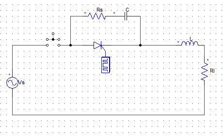
a) I(1 – e-t/τ)
b) I(1 + e-t/τ)
c) I(1 – et/τ)
d) I(1 + e-t/τ)
Answer: a
Explanation: As soon as the switch is closed, C acts like a S.C & the voltage equation gives
Vs = (Rs + Rl) I + L di/dt
Solve the above D.E.
6. The effect of over-voltages on SCR are minimized by using
a) RL circuits
b) Circuit breakers
c) Varistors
d) di/dt inductor
Answer: c
Explanation: Varistors are non-linear voltage clamping devices, RC circuits across the loads can also be used.
7. Over-current protection in SCRs is achieved through the use of
a) Varistors
b) Snubber Circuits
c) F.A.C.L.F & C.B.
d) Zener diodes
Answer: c
Explanation: FACLF stands for Fast Acting Current Limiting Fuse.
8. False triggering of the SCRs by varying flux & noise is avoided by using
a) F.A.C.L.F & C.B
b) Shielded cables & twisted gate leads
c) Snubber circuits
d) di/dt inductor in series with the gate terminal
Answer: b
Explanation: Shielded cables provide isolation from outside noise.
9. The thyristor has the following specifications
Vs = 400 V
(di/dt)max = 25 A/μsec
Find the value of L
a) 8 μH
b) 80 μH
c) 16 μH
d) 160 μH
Answer: c
Explanation: As soon as the switch is closed, C acts like a S.C & the voltage equation gives,
Vs = (Rs + Rl) I + L di/dt
Solve the above D.E.
di/dt = Vs/L e-t/τ
di/dt is maximum at t = 0, substitute the above given values & find L
10. Thyristors are used in electronic crowbar protection circuits because it possesses
a) high surge current capabilities
b) high amp 2-sec rating
c) less switching losses
d) voltage clamping properties
Answer: a
Explanation: Crowbar protection circuits have high surge current capabilities.
Thyristor Mounting
1. The usual way to accomplish higher gate current for improved di/dt rating is by using
a) varistors
b) pilot thyristors
c) twisted cables
d) op-amps
Answer: b
Explanation: Pilot SCR is an SCR which is fired which activates the firing circuit and fires the main SCR.
2. Inter-digitating of gate-cathode regions in SCR devices improves the
a) I2t rating
b) di/dt rating
c) dv/dt rating
d) thermal resistance
Answer: b
Explanation: Inter-digitating is the inter-mixing of the gate-cathode area to improve the di/dt ratings. di/dt rating is improved by providing more cathode conduction area during the delay and rise time.
3. The dv/dt rating of SCR can be improved by using
a) cathode-short structure
b) anode-short structure
c) gate-short structure
d) centre gate thyristor
Answer: a
Explanation: Cathode shorts are realized by overlapping metal on cathode n+ layers with a narrow p-region in between.
4. The total thermal resistance between junction and ambient θjA is 10°C/W. θjc is 2°C/W. θcs is 4°C/W. θsA = ?
a) 4°C/W
b) 2°C/W
c) 10°C/W
d) 16°C/W
Answer: a
Explanation: θjA = θjc+ θcs+ θsA.
5. Which of the following thermal resistance parameters depends on the size of the device and the clamping pressure?
a) θsA
b) θcs
c) θjc
d) None
Answer: b
Explanation: The case-to-sink thermal resistance depends on the size of the device, pressure, grease between the interface, etc.
6. The sink to ambient thermal resistance of SCR θsA
a) depends on the flatness of the device
b) depends on the length of the device
c) depends on the current carrying capabilities
d) is independent on thyristor configuration
Answer: d
Explanation: It does not depend on any of the device configurations.
7. Pav x (θjc + θcs + θsA) =
a) Maximum specified temperature
b) Energy lost
c) Difference in temperature between junction & ambient
d) Sum of junction & ambient temperature
Answer: c
Explanation: Pav = (Tj – Ta)/θjA
θjA = (θjc + θcs + θsA).
8. Heat dissipation from heat sink mainly takes place by
a) radiation
b) convection
c) absorption
d) none of the mentioned
Answer: b
Explanation: Heat DISSIPATION (rejection of heat to the atmosphere) takes place through convention only.
9. For low power SCRs (about 1 Ampere current) _____________ type of mounting is used
a) lead
b) stud
c) bolt-down
d) press-fit
Answer: a
Explanation: Lead mounting is a very simple time of mounting used for low power devices.
10. In the ___________ type of mounting the SCR is pressed between two heat sinks
a) bolt-down mounting
b) stud-mounting
c) press-pak mounting
d) cross-fit mounting
Answer: c
Explanation: In the press-pak type the device is pressed or clamped between two heat-sinks & external pressure is applied from both the sides.
Interconnecting Thyristors
1. SCRs are connected in parallel to fulfill the ___________ demand
a) high voltage
b) high current
c) size
d) efficiency
Answer: b
Explanation: Number of devices connected in parallel can carry huge amounts of current.
2. The term used to measure the degree of utilization of SCRs connected in series & parallel is
a) tuf
b) string efficiency
c) voltage/current utilization ratio
d) rectification efficiency
Answer: b
Explanation: String Efficiency = Rating of the whole string/(rating of one SCR x number of SCRs)
3. To have maximum possible string efficiency
a) SCRs of same rating must be used
b) SCRs with similar V-I characteristics must be used
c) SCRs with the same dimensions must be used
d) SCRs with similar thermal characteristics must be used
Answer: b
Explanation: Having similar ratings does not mean they have similar charc.
4. For a string voltage of 3300 V, let there be six series connected SCRs each of voltage 600V. Then the string efficiency is
a) 99.36 %
b) 91.7 %
c) 98.54 %
d) 96 %
Answer: c
Explanation: String efficiency = 3300/(6 x 600) = 98.54.
5. The measure of reliability of string is given by the factor
a) DRF = 1 – String efficiency
b) DRF = 1 + String efficiency
c) DRF = String efficiency – 1
d) DRF = String efficiency x 2
Answer: a
Explanation: DRF is de-rating factor given by the above expression.
6. When an extra SCR is connected in series with a string
a) DRF decreases
b) DRF increases
c) DRF remains constant
d) None of the mentioned
Answer: b
Explanation:
DRF = 1 – String efficiency
String Efficiency = Rating of the whole string/(rating of one SCR x number of SCRs)
Extra SCR will reduce the string efficiency which in turn increase the DRF.
7. The most practical way of obtaining a uniform distribution of series connected SCRs is to
a) connect a resistor of value R in series with each of the series connected SCRs
b) connect a resistor of value R in parallel with each of the series connected SCRs
c) connect a resistor of value R in series with one of the series connected SCRs
d) connect a resistor of value R in parallel with one of the series connected SCRs
Answer: b
Explanation: For uniform distribution of voltage across series connected SCRs, a resistor of value R in parallel with each series connected SCR.
8. 3 SCRs are connected in series. The string efficiency is 91%. SCRs 1, 2 & 3 have leakage currents 4 mA, 8 mA & 12 mA. Which SCR will block more voltage?
a) SCR-1
b) SCR-2
c) SCR-3
d) All the three will block equal voltage
Answer: a
Explanation: The SCR with lower leakage current block more voltage.
9. Two parallel connect SCRs have same voltage drop (Vt) having rated current = 2I1. SCR-1 carries a current of I1=2.6 A whereas SCR-2 carries a current of I2=1.4 A. Find the string efficiency.
a) 45 %
b) 77 %
c) 92 %
d) 84 %
Answer: b
Explanation: The total current would be I1+I2 & rated current is 2I1
String efficiency = (I1+I2)/2I1.
10. SCRs with a rating of 1000 V & 200 A are available to be used in a string to handle 6 KV & 1 KV. Calculate the number of series & parallel units required in case the de-rating factor is 0.1. (Round off the fraction to the greatest & nearest integer)
a) Series = 7, Parallel = 6
b) Series = 6, Parallel = 7
c) Series = 6, Parallel = 6
d) Series = 7, Parallel = 7
Answer: a
Explanation: DRF = 1-S.E
Therefore
0.1 = (1-6000/1000Ns) = (1-1000/200Np)
Ns = 6.6 = 7(say)
Np = 5.5 = 6(say)
Other Thyristor Members-1
1. _________ device from the thyristor family has its gate terminal connected to the n-type material near the anode.
a) SCR
b) RCT
c) PUT
d) SUT
Answer: c
Explanation: PUT is Programmable Unijunction Transistor which is a p-n-p-n device just like the SCR with its gate connected to the n-type material.
2. The Programmable Unijunction Transistor (PUT) turns on & starts conducting when the
a) gate voltage exceeds anode voltage by a certain value
b) anode voltage exceeds gate voltage by a certain value
c) gate voltage equals the anode voltage
d) gate is given negative pulse w.r.t to cathode
Answer: b
Explanation: The device only starts to conduct when the forward anode to cathode voltage exceeds the applied gate to cathode voltage.
3. The equivalent circuit of SUS (Silicon Unilateral Switch) consists of
a) a diode in series with a PUT
b) a diode in parallel with a PUT
c) a diode in anti-parallel with a PUT
d) two diodes
Answer: c
Explanation: It is a diode connected in anti-parallel with a PUT.
4. From the following list of devices, choose the device that only turns-on for a fixed-value of anode-cathode voltage
a) PUT
b) SCR
c) SUS
d) BJT
Answer: c
Explanation: Unlike the other devices the SUS only turns-on for a fixed value of anode to cathode voltage.
5. The SCS (Silicon Controlled Switch) is a
a) two terminal device
b) three terminal device
c) four terminal device
d) five terminal device
Answer: c
Explanation: The SCS is a four terminal device A,K,KG & AG.
6. The SCS is a four layer, four terminal thyristor. Can be turned on by
a) the anode gate
b) the cathode gate
c) either of the gates
d) gating both the gates together
Answer: c
Explanation: The SCS has two gates, anode-gate and cathode-gate. Either of the gates could be used to turn on the device.
7. The SCS (Silicon Controlled Switch) can be turned on by two methods, by applying __________ and __________
a) positive pulse to the anode gate, positive pulse to the cathode gate
b) positive pulse to the anode gate, negative pulse to the cathode gate
c) negative pulse to the anode gate, positive pulse to the cathode gate
d) negative pulse to the anode gate, negative pulse to the cathode gate
Answer: c
Explanation: Either of the gates could be used to turn on the device.
8. Which of the following devices provide complete isolation between triggering circuit and power circuit?
a) PUT
b) LASCR
c) SUS
d) DIAC
Answer: b
Explanation: Complete Isolation between triggering circuit & power circuit is the major advantage of using LASCR as they are light activated or light trigged.
9. The DIAC can be represented by
a) two SCRs in anti-parallel
b) two SCRs in parallel
c) two diodes in anti-parallel
d) two diodes in parallel
Answer: c
Explanation: The DIAC is nothing but a bi-directional diode.
10. The TRIAC can be represented by
a) two SCRs in anti-parallel
b) two SCRs in parallel
c) two diodes in anti-parallel
d) two diodes in parallel
Answer: a
Explanation: The TRIAC is a bidirectional SCR.
Other Thyristor Members-2
1. The SITH (Static Induction Thyristor) is a
a) 4 terminal, self-controlled device
b) 3 terminal, self-controlled device
c) 4 terminal, un-controllable device
d) 3 terminal, un-controllable device
Answer: b
Explanation: It is just like a GTO but it is p-n-n device.
2. The SITH has
a) gate, anode, cathode
b) base, collector, emitter
c) base, anode, cathode
d) gate, emitter, collector
Answer: a
Explanation: The SITH has 3 terminals viz. gate, anode and cathode.
3. The SITH is a
a) p+ n+ diode with p+ electrodes
b) n+ p+ n– diode with p+ electrodes
c) p+ n n+ diode with p+ electrodes
d) p n+ p+ n with p+ electrodes
Answer: c
Explanation: The Static Induction Thyristor is a p+ n+ diode with p+ electrodes.
4. The SITH is a
a) normally-off device
b) normally-on device
c) uncontrollable device
d) none of the mentioned
Answer: b
Explanation: The SITH unlike other devices is a normally on-device which can be switched off as and when required.
5. The SITH will act as a diode when the
a) anode is forward biased with zero gate-cathode voltage
b) anode is reversed biased with zero gate-cathode voltage
c) anode is forward biased and a positive gate voltage is applied
d) anode is forward biased and a negative gate voltage is applied
Answer: a
Explanation: Load current flows from anode to cathode as the p+ junction is forward biased.
6. In SITH, the magnitude of the anode current can be controlled by
a) controlling the anode-cathode voltage
b) controlling the negative gate bias
c) controlling the positive gate bias
d) it cannot be controlled
Answer: b
Explanation: Controlling the negative gate bias controls the main anode current.
7. The SITH
a) has high reverse blocking capabilities as compared to CTs
b) has low reverse blocking capabilities as compared to CTs
c) has no reverse blocking capabilities
d) none of the mentioned
Answer: c
Explanation: It has no reverse blocking capabilities due to emitter-shorting.
8. The TRIAC’s terminals are
a) gate, anode, cathode
b) MT1, MT2, gate
c) gate1, gate2, anode, cathode
d) MT1, MT2, gate1, gate2
Answer: b
Explanation: TRAIC has MT1, MT2 and a gate.
9. The RCT (Reverse Conducting Thyristor) has
a) a diode in series with the SCR
b) a diode in anti-parallel with the SCR
c) two SCR’s in anti-parallel
d) none of the mentioned
Answer: b
Explanation: A diode in anti-parallel with the SCR is called as a RCT.
10. The TRIAC is most sensitive in the _________ quadrants
a) 1st & 3rd with positive gate current
b) 1st with positive gate current & 3rd with negative gate current
c) 3st with positive gate current & 1rd with negative gate current
d) 1st & 3rd with negative gate current
Answer: b
Explanation: It is the most sensitive when all the voltage,current and gate signal have the same polarities.
GTOs
1. The GTO (gate turn-off thyristor) is a
a) p-n-p-n device
b) p-n-p device
c) p-metal-n device
d) p-n single junction device
Answer: a
Explanation: Just like a SCR, the GTO is a four layer p-n-p-n device.
2. The GTO can be turned off
a) by a positive gate pulse
b) by a negative gate pulse
c) by a negative anode-cathode voltage
d) by removing the gate pulse
Answer: b
Explanation: The GTO can be turned off by applying a negative gate pulse to the gate terminal.
3. The anode current is ideally limited by the
a) gate pulse amplitude
b) internal impedance of the device
c) load Impedance
d) gate circuit impedance
Answer: c
Explanation: The SCR or any device is connected through the load, hence the magnitude of the anode current (same as load current) will depend on the supply voltage and load impedance.
4. In a GTO the n+ layer forms the
a) anode & gate
b) cathode & gate
c) cathode
d) gate
Answer: c
Explanation: The bottom n+ layer forms the cathode.
5. The turn-off gain βoff of the GTO is given by
a) Ig/Ia
b) Ia/Ig
c) Vg/Va
d) Vg/Va
Answer: b
Explanation: βoff = (anode current/gate current).
6. A GTO can be represented by two transistors T1 & T2. The current gain of both transistors are α1 and α2 respectively. A low value of gate current requires
a) low value of α1 and α2
b) low value of α1 and high value of α2
c) high value of α1 and low value of α2
d) high values of α1 and α2
Answer: b
Explanation: In order that the gate current for turning-off the device is low, α2 should be made as nearer to unity as possible whereas α1 should be small.
7. Gold doped GTOs have _____________ as compared to the conventional GTOs
a) high turn-off time
b) low negative gate current requirement
c) low reverse voltage blocking capabilities
d) lower positive gate current requirement
Answer: b
Explanation: Gold doping reduces the negative gate current requirements, different kinds of dopings have different advantages over the others.
8. Latching current for the GTOs is ________ as compared to CTs (Conventional thyristors).
a) more
b) less
c) constant
d) cannot be said
Answer: a
Explanation: Latching current of GTOs is 2-4A as compared to 200 to 400 mA in case of CT’s.
9. In case of the two-transistor model (T1 & T2) of GTO with anode-short, the anode-short is placed between the
a) emitter of T1 & T2
b) emitter of T1 & base of T2
c) emitter of T1 & base of T1
d) emitter of T1 & collector of T2
Answer: c
Explanation: Draw the model. The anode-short resistor is connected between emitter (Anode A of GTO) with base of T1 transistor.
10. Choose the correct statement:
GTOs have _________ as compared to the CTs.
a) less on-state voltage drop
b) less gate drive losses
c) higher reverse blocking capabilities
d) faster switching speed
Answer: d
Explanation: GTOs have less turn-on and turn-off time, making it efficient for high frequency applications.