Up To Date Operational Amplifier MCQs ( Linear Integrated Circuits ) MCQs – Linear Integrated Circuits MCQs

Latest Linear Integrated Circuits MCQs
By practicing these MCQs of Operational Amplifier MCQs ( Linear Integrated Circuits ) MCQs – Latest Competitive MCQs , an individual for exams performs better than before. This post comprising of objective questions and answers related to “Operational Amplifier MCQs ( Linear Integrated Circuits ) Mcqs “. As wise people believe “Perfect Practice make a Man Perfect”. It is therefore practice these mcqs of Linear Integrated Circuits to approach the success. Tab this page to check “Operational Amplifier MCQs ( Linear Integrated Circuits )” for the preparation of competitive mcqs, FPSC mcqs, PPSC mcqs, SPSC mcqs, KPPSC mcqs, AJKPSC mcqs, BPSC mcqs, NTS mcqs, PTS mcqs, OTS mcqs, Atomic Energy mcqs, Pak Army mcqs, Pak Navy mcqs, CTS mcqs, ETEA mcqs and others.
Operational Amplifier MCQs ( Linear Integrated Circuits ) MCQs – Linear Integrated Circuits MCQs
The most occurred mcqs of Operational Amplifier MCQs ( Linear Integrated Circuits ) in past papers. Past papers of Operational Amplifier MCQs ( Linear Integrated Circuits ) Mcqs. Past papers of Operational Amplifier MCQs ( Linear Integrated Circuits ) Mcqs . Mcqs are the necessary part of any competitive / job related exams. The Mcqs having specific numbers in any written test. It is therefore everyone have to learn / remember the related Operational Amplifier MCQs ( Linear Integrated Circuits ) Mcqs. The Important series of Operational Amplifier MCQs ( Linear Integrated Circuits ) Mcqs are given below:
Differential Amplifier and Circuit Configuration
1. A Differential Amplifier should have collector resistor’s value (RC1 & RC2) as
a) 5kΩ, 5kΩ
b) 5Ω, 10kΩ
c) 5Ω, 5kΩ
d) 5kΩ, 10kΩ
Answer: a
Explanation: The values of collector current will be equal in differential amplifier (RC1=RC2).
2. A Differential Amplifier amplifies
a) Input signal with higher voltage
b) Input voltage with smaller voltage
c) Sum of the input voltage
d) None of the Mentioned
Answer: d
Explanation: The purpose of differential amplifier is to amplify the difference between two signals.
3. The value of emitter resistance in Emitter Biased circuit are RE1=25kΩ & RE2=16kΩ. Find RE
a) 9.756kΩ
b) 41kΩ
c) 9.723kΩ
d) 10kΩ
Answer: a
Explanation: In emitter biased circuit, RE1 & RE2 is connected in parallel combination.
⇒ RE = RE1 II RE2 = (RE1× RE2)/(RE1+RE2) = (25kΩ×16kΩ)/(25kΩ+16kΩ) = 9.7561kΩ.
4. If output is measured between two collectors of transistors, then the Differential amplifier with two input signal is said to be configured as
a) Dual Input Balanced Output
b) Dual Input Unbalanced Output
c) Single Input Balanced Output
d) Dual Input Unbalanced Output
Answer: a
Explanation: When two input signals are applied to base of transistor, it is said to be Dual Input. When both collectors are at same DC potential with respect to ground, then it is said to be Balance Output.
5. A differential amplifier is capable of amplifying
a) DC input signal only
b) AC input signal only
c) AC & DC input signal
d) None of the Mentioned
Answer: c
Explanation: Direct connection between stages removes the lower cut off frequency imposed by coupling capacitor; therefore it can amplify both AC and DC signal.
6. In ideal Differential Amplifier, if same signal is given to both inputs, then output will be
a) Same as input
b) Double the input
c) Not equal to zero
d) Zero
Answer: d
Explanation: In ideal amplifier, Output voltage
⇒ Vout = Vin1-Vin2.
7. Find the Single Input Unbalance Output configuration in following circuit diagrams :
a) 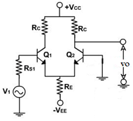
b) 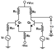
c) 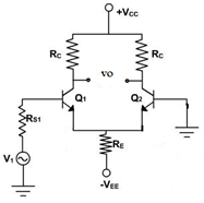
d) 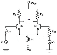
Answer: c
Explanation: Circuit c has only single input (V1) and output is measure only at one of the collector with respect to ground.
8. An emitter bias Dual Input Balanced Output differential amplifier has VCC=20v, β=100, VBE=0.7v, RE=1.3kΩ. Find IE
a) 7.42mA
b) 9.8mA
c) 10mA
d) 8.6mA
Answer: a
Explanation: Emitter current can be found out by substituting the values in the equation,
⇒ IE = (VEE-VBE)/(2RE) = (20v-07v)/(2×1.3kΩ) = 7.42mA.
9. Find IC, given VCE=0.77v, VCC=10v, VBE=0.37v and RC=2.4kΩ in Dual Input Balanced Output differential amplifier
a) 0.4mA
b) 0.4A
c) 4mA
d) 4A
Answer: c
Explanation: Substitute the values in collector to emitter voltage equation,
VCE= VCC+ VBE-RC IC
⇒IC = (VCC-VCE+VBE)/RC = (10v-0.77v+0.37v)/2.4kΩ = 4mA
10. Find the correct match
| Configuration | Voltage gain and Input resistance |
|---|---|
| 1. Single Input Unbalanced Output | i. Ad = Rc/re , Ri1 Ri2 = 2βacRE |
| 2. Dual Input Balanced Output | ii. Ad= Rc/2re , Ri1 Ri2 = 2βacRE |
| 3. Single Input Balanced Output | iii. Ad= Rc/re , Ri = 2βacRE |
| 4. Dual Input Unbalanced Output | iv. Ad = Rc/2re , Ri = 2βacRE |
a) 1-i , 2-iii, 3-iv, 4-ii
b) 1-iv, 2-ii, 3-iii, 4-i
c) 1-ii, 2-iv, 3-i , 4-iii
d) 1-iii, 2-i, 3-ii, 4-iv
Answer: d
Explanation: Properties of differential amplifier circuit configuration.
11. Obtain the collector voltage, for collector resistor (RC) =5.6kΩ, IE=1.664mA and VCC=10v for single input unbalanced output differential amplifier
a) 0.987v
b) 0.682v
c) 0.555v
d) None of the mentioned
Answer: b
Explanation: Substitute the given values in collector voltage equation,
VC= VCC – RC×IC
⇒ VC= 10v – 5.6kΩ×1.664mA (∵ IC ≅ IE )
⇒ VC= 0.682v.
12. For the circuit shown below, determine the Output voltage (Assume β=5, differential input resistance=12 kΩ)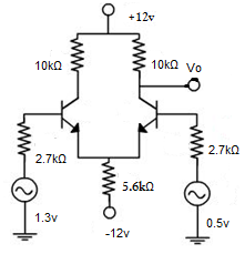
a) 4.33v
b) 2.33v
c) 3.33v
d) 1.33v
Answer: c
Explanation: From the circuit dig, RC=10kΩ, Vin1= 1.3v and Vin2=0.5v,
Differential input resistance = 2 βre,
⇒ 12kΩ = 2×5×Re
⇒ Re = 1.2 kΩ
Output voltage Vo = RC/2Re(Vin1-Vin2)
⇒ Vo = 10kΩ/(2 ×1.2kΩ) × (1.3v-0.5v)
⇒ Vo = 3.33v.
13. In a Single Input Balanced Output Differential amplifier, given VCC=15v, RE = 3.9kΩ, VCE=2.4 v and re=250Ω. Determine Voltage gain
a) 26
b) 56
c) 38
d) 61
Answer: a
Explanation: In single Input Balance Output amplifier,
⇒ IE = (VEE-VBE)/2RE
=(15v-0.7v)/(2×3.9kom)= 1.83mA (∵VCC=VEE)
From the equation, VCE = VCC +VBE-RC×IC
⇒ RC = (14.3v – 2.4v)/1.83mA = 6.5kΩ
The voltage gain, Vo
⇒ Vo = RC/re
= 6.5kΩ/250Ω = 26(no units).
Operational Amplifier Internal Circuit – 1
1. Which is not the internal circuit of operational amplifier?
a) Differential amplifier
b) Level translator
c) Output driver
d) Clamper
Answer: d
Explanation: Clamper is an external circuit connected at the output of Operational amplifier, which clamp the output to desire DC level.
2. The purpose of level shifter in Op-amp internal circuit is to
a) Adjust DC voltage
b) Increase impedance
c) Provide high gain
d) Decrease input resistance
Answer: a
Explanation: The gain stages in Op-amp are direct coupled. So, level shifter is used for adjustment of DC level.
3. How a symmetrical swing is obtained at the output of Op-amp
a) Providing amplifier with negative supply voltage
b) Providing amplifier with positive voltage
c) Providing amplifier with positive& negative voltage
d) None of the mentioned
Answer: c
Explanation: For example, consider a single voltage supply +15v. During positive half cycle the output will be +5v and -10v during negative half cycle.
Therefore, the maximum peak to peak output swing, -5v (-10v) = -15v (Asymmetrical swing).
So, to get symmetrical swing both positive and negative supply voltage with bias point fixed suitably is required.
4. What is the purpose of differential amplifier stage in internal circuit of Op-amp?
a) Low gain to differential mode signal
b) Cancel difference mode signal
c) Low gain to common mode signal
d) Cancel common mode signal
Answer: d
Explanation: Any undesired noise, common to both of the input terminal is suppressed by differential amplifier.
5. Which of the following is not preferred for input stage of Op-amp?
a) Dual Input Balanced Output
b) Differential Input Single ended Output
c) Cascaded DC amplifier
d) Single Input Differential Output
Answer: c
Explanation: Cascaded DC amplifier suffers from major problem of drift of the operating point, due to temperature dependency of the transistor.
6. What will be the emitter current in a differential amplifier, where both the transistor are biased and matched? (Assume current to be IQ)
a) IE = IQ/2
b) IE = IQ
c) IE = (IQ)2/2
d) IE = (IQ)2
Answer: a
Explanation: Due to symmetry of differential amplifier circuit, current IQ divides equally through both transistors.
7. From the circuit, determine the output voltage (Assume αF=1)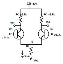
a) VO1=3.9v , VO2=12v
b) VO1=12v , VO2=3.9v
c) VO1=12v , VO2=0v
d) VO1=3.9v , VO2=-3.9v
Answer: b
Explanation: The voltage at the common emitter ‘E’ will be -0.7v, which make Q1 off and the entire current will flow through Q2.
⇒ VO1 = VCC VO2= VCC-αF×IQ×RC,
⇒ VO1 = 12v , VO2=12v-1×3mA×2.7k = 3.9v.
8. At what condition differential amplifier function as a switch
a) 4VT < Vd < -4VT
b) -2VT ≤ Vd ≤ 2VT
c) 0 ≤ Vd < -4VT
d) 0 ≤ Vd ≤ 2VT
Answer: a
Explanation: For Vd > 4VT, the output voltage are VO1 = VCC, VO2= VCC-αF IQRC. Therefore, a transistor Q1 will be ON and Q2 will be OFF. Similarly for Vd> -4VT, both transistors Q2 & Q1 will be ON.
9. For Vd > ±4VT, the function of differential amplifier will be
a) Switch
b) Limiter
c) Automatic gain control
d) Linear Amplifier
Answer: b
Explanation: At this condition, input voltage of the amplifier is greater than ±100mv and thus acts as a limiter.
10. Change in value of common mode input signal in differential pair amplifier make
a) Change in voltage across collector
b) Slight change in collector voltage
c) Collector voltage decreases to zero
d) None of the mentioned
Answer: a
Explanation: In differential amplifier due to symmetry, both transistors are biased and matched. Therefore, Voltage at each collector will be same.
11. Find collector current IC2, given input voltages are V1=2.078v & V2=2.06v and total current IQ=2.4mA. (Assume α=1)
a) 0.8mA
b) 1.6mA
c) 0.08mA
d) 0.16mA
Answer: a
Explanation: Collector current, IC2=αF×IQ/(1+eVd⁄VT),
VT = Volts equivalent of temperature = 25mv,
⇒ Vd = V1-V2 =2.078v-2.06v=0.018v (equ1)
Substituting equation 1,
⇒ Vd/VT = 0.018v/25mv = 0.72v (equ2)
Substituting equation 2,
⇒ IC2= 1×2.4mA/(1+e0.72) = 2.4mA/(1+2.05) = 0.8mA.
12. A differential amplifier has a transistor with β0= 100, is biased at ICQ = 0.48mA. Determine the value of CMRR and ACM, if RE =7.89kΩ and RC = 5kΩ.
a) 49.54 db
b) 49.65 d
c) 49.77 db
d) 49.60 db
Answer: b
Explanation: Differential mode gain, ADM= -gmRC and Common mode gain,
⇒ ACM= -(gmRC)/(1+2gmRE)
(for β0≫1).
Substituting the values,
⇒ gm= ICQ/VT = 0.48mA/25mv=19.2×10-3Ω-1
⇒ ADM= -gm×RC= -19.2×10⁻³Ω-1×5kΩ= -96
⇒ ACM= -(gmRC)/(1+2gmRE)= -(19.2×10⁻³Ω-1×5kΩ) /(1+2×-⇒ 19.2×10⁻³Ω-1×7.89kΩ) = -0.3158
CMRR = -96/-0.3158= 303.976
=20log303.976
=49.65db
Operational Amplifier Internal Circuit – 2
1. How are the arbitrary signal represented, that are applied to the input of transistor? (Assume common mode signal and differential mode signal to be VCM & VDM respectively).
a) Sum of VCM & VDM
b) Difference of VCM & VDM
c) Sum and Difference of VCM & VDM
d) None of the mentioned
Answer: c
Explanation: In practical situation, arbitrary signal are signal are represented as Sum and Difference of common mode signal and differential mode signal.
2. How the differential mode gain is expressed using ‘h’ parameter for a single ended output?
a) – hfeRC/hie
b) 1/2×(hfeRC)/hie
c) – 1/2×hfeRC
d) None of the mentioned
Answer: b
Explanation: Formula for differential mode gain using ‘h’ parameter model for a single ended output.
3. Find Common Mode Rejection Ration, given gm =16MΩ-1, RE=25kΩ
a) 58 db
b) 40 db
c) 63 db
d) 89 db
Answer: a
Explanation: Formula for Common Mode Rejection Ration, CMRR= 1+2gmRE,
⇒ CMRR = 1+(2×16MΩ-1×25kΩ)
= 801 = 20log801 = 58.07 db.
4. In differential amplifier the input are given as V1=30sinΠ(50t)+10sinΠ(25t) , V2=30sinΠ(50t)-10 sinΠ(25t), β0 =200,RE =1kΩ and RC = 15kΩ. Find the output voltages V01, V02 & gm=4MΩ-1
a) V01=-60[10 sinΠ(25t) ]-6.637[30sinΠ(50t) ], V02=60[10 sinΠ(25t) ]-6.637[30sinΠ(50t) ].
b) V01=-6.637[10 sinΠ(25t) ]-60[30sinΠ(50t) ], V02=6.637[10 sinΠ(25t) ]-60[30sinΠ(50t) ].
c) V01=-60[30 sinΠ(50t) ]-6.637[10sinΠ(25t) ], V02=60[30 sinΠ(50t) ]-6.637[10sinΠ(25t) ].
d) V01=-6.637[30 sinΠ(50t) ]-60[10sinΠ(25t) ], V02=6.637[30 sinΠ(50t) ]-60[10sinΠ(25t) ].
Answer: a
Explanation: Differential mode gain, ADM = -gm RC,
⇒ ADM = -4MΩ-1×15kΩ = 60
⇒ rΠ=β0/gm =200/4MΩ-1 =50kΩ
Common mode gain, ACM=-βo×RC/rΠ+(βO+1)×RE
⇒ ACM =-200×15kΩ/50kΩ+2(1+200)×1kΩ=-6.637
Common mode signal, VCM=(V1+V2)/2= 30sinΠ(50t)
Differential mode signal, VDM=(V1-V2)/2= 10 sinΠ(25t)
Output voltages are given as
⇒ V01=ADM)× VDM)+ ACM× VCM
= -60[10 sinΠ(25t)]-6.637[30sinΠ(50t)],
⇒ V02=-ADM× VDM+ ACM× VCM
= 60[10 sinΠ(25t)]-6.637[30sinΠ(50t)].
5. If the value of Common Mode Rejection Ratio and Common Mode Gain are 40db and -0.12 respectively, then determine the value of differential mode gain
a) 0.036
b) -1.2
c) 4.8
d) 12
Answer: d
Explanation: Common mode rejection ratio, CMRR =log-1×(40/20) = 100
⇒ CMRR =(∣ADM∣/ ∣ACM∣)
⇒ ∣ADM∣ =100×0.12 = 12.
6. To increase the value of CMRR, which circuit is used to replace the emitter resistance Re in differential amplifier?
a) Constant current bias
b) Resistor in parallel with Re
c) Resistor in series with Re
d) Diode in parallel with Re
Answer: a
Explanation: Constant current bias offers extremely large resistor under AC condition and thus provide high CMRR value.
7. What is the purpose of diode in differential amplifier with constant current circuit?
a) Total current independent on temperature
b) Diode is dependent of temperature
c) Transistor is depend on temperature
d) None of the mentioned
Answer: a
Explanation: The base emitter voltage of transistor (VBE) in constant current circuit by 2.5mv/oc, thus diode also has same temperature. Hence two variations cancel each other and total current IQ become in depend of temperature.
8. How to improve CMRR value
a) Increase common mode gain
b) Decrease common mode gain
c) Increase Differential mode gain
d) Decrease differential mode gain
Answer: b
Explanation: For a large CMRR value, ACM should be small as possible.
9. Define total current (IQ) equation in differential amplifier with constant current bias current
a) IQ=1/R3×(VEE/R1+R2)
b) IQ =(VEE×R2)/(R1+R2)
c) IQ=1/R3×(VEE×R2/R1+R2)
d) IQ)=R3×(VEE/R1+R2)
Answer: c
Explanation: The equation for total current is obtained by applying Kirchhoff’s Voltage Law to constant current circuit in differential amplifier.
10. Constant current source in differential amplifier is also called as
a) Current Mirror
b) Current Source
c) Current Repeaters
d) All of the mentioned
Answer: a
Explanation: The output current is reflection or mirror of the reference input current. Therefore, the constant current source circuit referred as Current Mirror.
11. When will be the mirror effect valid
a) β≫1
b) β=1
c) β<1
d) β≠1
Answer: a
Explanation: If value of β is used in the equation, IC=β/(β+2)×Iref. It almost become unity and the output current become equal to reference current.
12. Calculate the value of reference current and input resistor for current mirror with IC=1.2μA & VCC=12v. Assume β=50.
a) 1.248mA, 9kΩ
b) 1.248mA, 9.6kΩ
c) 1.248mA, 9.2kΩ
d) 1.2mA, 9.6kΩ
Answer: a
Explanation: We know that collector current, IC=β/(β+2)×Iref,
⇒ Iref=(β+2)/β×IC= (50+2)/50× 1.2μA = 1.248mA
⇒ Iref=(VCC-VBE)/R1
⇒ R1=(12v-07v)/1.248mA = 9.05kΩ.
Operational Amplifier Internal Circuit – 3
1. Determine the early voltage, if the output resistance is 2.5×2kΩ and input current is 2mA
a) 9.8v
b) 5.6v
c) 7.8v
d) 10v
Answer: d
Explanation: Output resistance, Ro=VA/Iref
⇒ VA = Ro×Iref =2.5×2kΩ×2mA =10v.
2. In practical application of current mirror, early voltage is assumed to be
a) Infinite
b) Zero
c) Unity
d) None of the mentioned
Answer: a
Explanation: Early voltage is assumed to be infinity, so that output resistance tend to infinity and the output current is constant.
3. A widlar current source is used
a) to get low value of current
b) to get high value of CMRR
c) to get low voltage of gain
d) to get high value of Output
Answer: a
Explanation: In the widlar current source Re is added to emitter lead of transistor, which consequently results in smaller output current value.
4. What will be the value of emitter resistance in widlar current source for output current 10mA, having Iref=2.7A
a) 67/(1+1/β)Ω
b) 13/(1+1/β)Ω
c) 14/(1+1/β)Ω
d) 1.36/(1+1/β)Ω
Answer: c
Explanation: Emitter resistor, RE=VT/(1+1/β) Iref×ln(Io/Iref)
⇒ RE= 0.025/(1+1/β)10mA × ln(12.7A/10mA) = 14/(1+1/β)Ω.
5. A current repeater having identical transistor has collector current, IC1 =0.39mA. Find IC2,IC4& IC6
a) 0.39mA, 0.39mA, 0.78mA
b) 0.78mA, 0.39mA, 0.39mA
c) 0.39mA, 0.78mA, 0.39mA
d) None of the mentioned
Answer: d
Explanation: In current repeater, the current IC = IC1 =IC2 =⋯= IC N≅ Iref . Where, N – Number of transistors used in current repeater circuit.
6. If the reference and collector current are 0.539mA and 0.49mA respectively, how many transistors are used in current repeater circuit? (Assume β =150)
a) 11
b) 14
c) 10
d) 8
Answer: b
Explanation: The current equation is given as IC= Iref×β/(β+1+N)
⇒ 0.49mA= 0.539mA×150/(150+1+N)
⇒ N=14.
7. For the current repeater shown in the circuit, determine IC4 value, Where β = 75.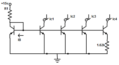
a) 0.035mA
b) 0.028mA
c) 0.04mA
d) 0.052mA
Answer: a
Explanation: The reference current, Iref = VCC-VBE/R1 =(15v-0.7v)/39kΩ = 0.366mA.
⇒ Iref=IC+4×IB
=IC(1+1/β)
∴ IC= Iref×(1+1/β)
=Iref×(1+1/β) = 0.366mA×(1+1/75) =0.347mA
⇒ IC1=IC2=IC3=0.347mA
To determine IC4,
RE=VT/(1+1/β)×IC4×ln(C3/IC4)
⇒ 1.62kΩ = 25mv/(1+1/75)×IC4×ln(0.347mA/IC4)
⇒ IC4=0.035mA (find using trial and error method).
8. The requirements for a good current source is the one in which, (Take Output current – IO and Output resistance – rO )
a) IO independent upon current gain and should be low
b) rO should be very high
c) IO in the circuit should be low
d) IO independent upon current gain and rO should be very high
Answer: d
Explanation: The need for high output resistance current source can be seen because the common mode gain of the differential amplifier can only be reduced by using high resistance current sources.
9. Which current source exhibits a very high output resistance?
a) Simple current mirror
b) Wilson current mirror
c) Widlar current mirror
d) All of the mentioned
Answer: b
Explanation: The output resistance of Wilson current mirror is substantially greater than ≅(β× Output resistance)/2 than Simple or Widlar current source.
10. What will be the overall gain in Darlington circuit, if the individual transistor gain is 200?
a) 10000
b) 40000
c) 8000
d) 1000
Answer: b
Explanation: Overall current gain, β= β1×β2 (Multiplication of current gain of individual transistor)
⇒ β=200×200=40000
11. To increase the input resistance in differential amplifier, replace the transistor by
a) Current mirror
b) Current repeater
c) Darlington pair
d) All of the mentioned
Answer: c
Explanation: Higher value of input resistance can be obtained by using Darlington pair in place of transistor.
12. What is the drawback in using Darlington pair in differential amplifier?
a) Large current gain
b) Output current in milli ampere
c) Gain is proportional to load resistor
d) High offset voltage
Answer: d
Explanation: Due to cascaded stage, Darlington differential amplifier offers higher offset voltage which is two times larger than ordinary two transistor used in differential amplifier.
13. Determine the amount of shift happens in level shifter?
a) Vcc + 0.7v
b) Vcc – 0.7v
c) -0.7v
d) +0.7v
Answer: c
Explanation: Level shifter is basically a simple type emitter follower. Hence, level shifter also act as a buffer to isolate high gain stages from the output stage. Therefore, the amount of shift obtained is
VO – Vi = -VBE = -0.7v.
Operational Amplifier Internal Circuit – 4
1. To increase the input resistance, the differential amplifier replaces transistor by
a) Current mirror
b) Current repeater
c) Darlington pair
d) All of the mentioned
Answer: c
Explanation: Higher value of input resistance can be obtained by using Darlington pair in place of transistor.
2. In Darlington pair differential amplifier the current gain is given as 100. Where IB1=5µA and IC1=0.35mA. Determine IC2
a) 0.5mA
b) 1.5mA
c) 2mA
d) 0.15mA
Answer: d
Explanation: The current gain in Darlington pair differential amplifier is given as β=( IC1+IC2)/IB1.
Substituting the values in the equation, we get
IC2=(β×IB1)-IC1 =(100×5µA)-0.35mA =0.15mA.
3. In the circuit shown, find the overall current gain?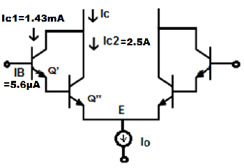
a) 456218
b) 444878
c) 444210
d) 455734
Answer: b
Explanation: From the circuit given, IB= IB1 = 5.6µA.
IE1= IB1+ IC1 = 1.43mA + 5.6µA = 1.435mA.
IE1= IB2 = 1.435mA.
The individual current gain values,
β1=IC1/ IB1
=> β1 = 1.43mA/5.6µA= 255.36.
Similarly,β2=IC2/ IB2
=> β2 = 2.5A / 1.435mA =1742.16
Therefore, the overall current gain, β = β1 × β2 = 255.36 × 1742.16 = 444878.
4. Introducing FET differential amplifier pair at the input stage of differential amplifier produces
a) High output resistance
b) High input resistance
c) Low input impedance
d) All of the mentioned
Answer: b
Explanation: Input resistance of the order 1012 Ω is possible with JFET at the input stage of differential amplifier.
5. Why active load is used in amplifier to obtain large gain in intermediate stage of amplifier?
a) To obtain a very large voltage gain
b) To get High input resistance
c) To reduce the noises
d) To increase current gain
Answer: a
Explanation: To increase gain usually large collector resistance value as gain is proportional to load resistor. However, due to limitation of maximum value load resistor, active loads are used in amplifier to obtain large gain in intermediate stages of amplifier.
6. Which circuit is used as active load for an amplifier
a) Wildar Current source
b) Darlington pair
c) Current Mirror
d) All of the mentioned
Answer: c
Explanation: Current mirror has DC resistance (order of few kΩ), as quiescent voltage across it is a fraction of supply voltage and current in milliampere.
7. What is the equation of load current for a differential amplifier with an active load?
a) IL = gm×vd
b) IL = Iq /2
c) IL = β×Iq×( Vin1 – Vin2)
d) IL = 2×gm/( Vin1 – Vin2)
Answer: a
Explanation: The load current is given as product of difference between input & output voltage and transconductance. Therefore, the equation of load current is ,
IL = gm×vd.
8. The input voltage of a difference amplifier are 2.5v and 4.9v. If the transconductance is 0.065Ω-1, determine the load current entering the next stage
a) 0.156A
b) 1.56A
c) 0.156mA
d) 15.6µA
Answer: a
Explanation: Load current entering the next stages of amplifier is the sum of individual load current, which is given by IL = IL1+ IL2 (Since only two input voltages are given).
IL = gm×Vin1 + gm×Vin2
= gm×( Vin1 – Vin2) = 0.065 Ω-1×(4.9v-2.5v) = 0.156A.
9. Calculate the VI – VO for the level shifter shown in the figure (Assume identical silicon transistor and very large value of β). Transistor QA and QB form current mirror.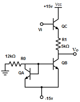
a) 5.56V
b) 6.00v
c) 7.98v
d) 6.65v
Answer: d
Explanation: Since the transistor QA and QB form current mirror, ICA= ICB = I.
=> I = (VCC – VBE) / R0 = (15v-0.7)/12k Ω (for β>>1, output current =input current)
=> I= 1.19mA.
The shift in level is given as VI – VO = VBE + I×R1 =0.07v+1.19mA×5kΩ =6.65v.
10. Load resistors (Re) is neglected for maximizing the voltage gain in amplifier because,
a) Requires large chip are
b) Requires large power supply
c) Quiescent drop across Re increases
d) All of the mentioned
Answer: d
Explanation: As gain is proportional to load resistor, large resistance value is required. Due to limitation mentioned, it is neglected.
11. What is the need for level shifter in operational amplifier?
a) Level the quiescent voltage
b) Remove distortion at output
c) Limits the output voltage
d) Increase the quiescent voltage
Answer: c
Explanation: Because of direct couple, Dc level rises stages to stage and tends to shift operating point. This limits output swing (Voltage).
12. Limitation of an output stage amplifier, if it emitter follower with complementary transistor
a) Cross-over distortion
b) Low impedance output
c) Shift in level
d) Active load current
Answer: a
Explanation: The limitation in the amplifier is that , the output voltage remains zero until the input voltage exceeds cut in voltage VBE= 0.5v, which is known as cross-over distortion.
13. An output stage amplifier can produce output signal, when the input signal is
a) 0.48v
b) 0.9v
c) 1.2v
d) 0.5v
Answer: c
Explanation: In an Output stage amplifier, due to cross-over distortion output voltage produces input voltage is greater than two times of cut-in voltage which is equal to 1v.
Since, VBE= 0.5v
=> 2×VBE= 1v.
14. Find the disadvantage in the following circuit diagram: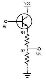
a) Voltage get attenuated by R1
b) Voltage get attenuated by R2
c) Voltage get attenuated by R1 and R2
d) Voltage shift get increased by the drop across R1 and R2
Answer: b
Explanation: The output taken at the junction of R1 and R2 increases the voltage shift. However, the disadvantage is that, the signal voltage gets attenuated by R2.
=> R2/(R1 + R2).