Updated Linear Integrated Circuits MCQs – New IC FABRICATION MCQs ( Linear Integrated Circuits ) MCQs

Latest Linear Integrated Circuits MCQs
By practicing these MCQs of IC FABRICATION MCQs ( Linear Integrated Circuits ) MCQs – Latest Competitive MCQs , an individual for exams performs better than before. This post comprising of objective questions and answers related to “IC FABRICATION MCQs ( Linear Integrated Circuits ) Mcqs “. As wise people believe “Perfect Practice make a Man Perfect”. It is therefore practice these mcqs of Linear Integrated Circuits to approach the success. Tab this page to check “IC FABRICATION MCQs ( Linear Integrated Circuits )” for the preparation of competitive mcqs, FPSC mcqs, PPSC mcqs, SPSC mcqs, KPPSC mcqs, AJKPSC mcqs, BPSC mcqs, NTS mcqs, PTS mcqs, OTS mcqs, Atomic Energy mcqs, Pak Army mcqs, Pak Navy mcqs, CTS mcqs, ETEA mcqs and others.
IC FABRICATION MCQs ( Linear Integrated Circuits ) MCQs – Linear Integrated Circuits MCQs
The most occurred mcqs of IC FABRICATION MCQs ( Linear Integrated Circuits ) in past papers. Past papers of IC FABRICATION MCQs ( Linear Integrated Circuits ) Mcqs. Past papers of IC FABRICATION MCQs ( Linear Integrated Circuits ) Mcqs . Mcqs are the necessary part of any competitive / job related exams. The Mcqs having specific numbers in any written test. It is therefore everyone have to learn / remember the related IC FABRICATION MCQs ( Linear Integrated Circuits ) Mcqs. The Important series of IC FABRICATION MCQs ( Linear Integrated Circuits ) Mcqs are given below:
Integrated Circuits, Types & Manufacturer’s Design – 1
1) What is the best choice of IC package used for experimental purpose?
a) DIP package
b) Metal can package
c) Flat pack
d) Transistor pack
Answer: a
Explanation: DIP package are used as it is easy to mount. The mounting does not require bending or soldering of the leads.
2. What is the general information specified in ordering an IC?
a) Temperature range
b) Device type
c) Package type
d) All of the mentioned
Answer: d
Explanation: Generally, in ordering an IC, all the three informations must be specified.
3. Find the ordering information for µA741TC.
a) Sprague 741 DIP with Industrial temperature range
b) Intersil 741 DIP with commercial temperature range
c) Fairchilds 741 DIP with commercial temperature range
d) Texas instrument 741 metal can with Industrial temperature range
Answer: c
Explanation: Here “µA” represents the identifying initials used by Fairchild,
T represents Mini DIP package and C represents Commercial temperature range.
4. How a Motorola IC with plastic DIP and commercial temperature range is ordered?
a) ICLxxxP -> 0o to 75oc
b) CAxxE -> -55o to +125oc
c) LMxxxxA -> -40o to+85oc
d) MCxxxP -> 0o to 70oc
Answer: d
Explantion: The ordering format for a typical Motorola IC is,
MCxxxx –> Device type
P –> Package type(Plastic DIP)
0o to 70oc –> Temperature range (Commercial).
5. What does the 1-2-3 numbering system used in National Semiconductor IC denotes
a) Validity in years
b) Temperature range
c) Package type
d) Ordering information
Answer: c
Explanation: In National linear ICs, a 1-2-3 numbering system is used to represent the temperature range.
6. How does a industrial temperature range device in National Semiconductor IC is represented?
a) LM305
b) LM101
c) LM201
d) All of the mentioned
Answer: c
Explanation: In LM201, the number 2 denotes an industrial temperature range device.
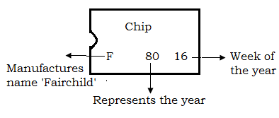
7. Use device identification method to find the IC of Fairchild chip manufactured in the year 1980.
Explanation: In the chip, 80 represent the manufactured year
8. Dual-In-Line pack is considered to be suitable for mounting because,
a) Easy to handle
b) Fits mounting hardware
c) Inexpensive
d) All of the mentioned
Answer: c
Explanation: DIP pack is easy to handle, fit standard mounting hardware and is inexpensive when moulded on plastic.
9. What is the use of notch and dot in DIP ICs?
a) Determine the pin configuration
b) Designed to represent device type
c) Represent property of IC
d) Find the pin number
Answer: d
Explanation: A notch and dot as viewed form top view is used to find the pin terminal. The terminals are numbered counter clockwise.
10. How an eight pin Dual-In-Line Package is shortly named
a) 8p DIP
b) Maxi DIP
c) Mini DIP
d) ES DIP
Answer: c
Explanation: An eight pin Dual-In-Line Package is called as Mini DIP as it is used for devices with minimum number of inputs and outputs.
Integrated Circuits, Types & Manufacturer’s Design – 2
1. Which package type is chosen for military purposes?
a) Ceramic DIP
b) Plat pack
c) Metal can pack
d) Plastic DIP
Answer: a
Explanation: Ceramic DIP can be used for high temperature and high performance equipment.
2. A Dual-In-Line Package is usually referred to as
a) DIPn
b) nDIP
c) DIPn
d) All of the mentioned
Answer: a
Explanation: A Dual-In-Line Package is usually referred to as DIPn. Where, n represent the number of pin terminals in the IC.
3. Which type of DIP IC dissipates more heat?
a) Ceramic DIP
b) Plastic DIP
c) Metal DIP
d) None of the mentioned
Answer: b
Explanation: Plastic DIP are cheaper than metal or ceramic DIP, but are not regarded as satisfactory in extremes of temperature.
4. Choose the type of package used for Airborne application?
a) DIP package
b) Metal can package
c) Flat pack
d) Transistor pack
Answer: c
Explanation: The flat pack is more reliable and lighter than a comparable DIP package and therefore is suited for airborne application.
5. How a choice is made, if all three package types are available?
a) Based on cost
b) Based on fabrication
c) Based on Experimentation usage
d) All of the mentioned
Answer: d
Explanation: When all three packages are available for a specific application, the choice can be made based on the relative cost, ease of fabrication and breadbording the IC.
6. How many temperature grades are available for IC?
a) Two
b) Three
c) Four
d) Five
Answer: b
Explanation: All ICs manufactured fall into one of the three basic temperature grades. They are military, industrial and commercial temperature range.
7. ICs used for industrial application will have temperature range from
a) -55o to +85oc
b) 90o to 155oc
c) 10o to 100oc
d) -20o to +85oc
Answer: d
Explanation: The industrial temperature range is from -20o to +85oc.
8. Find the types of temperature range used for an IC, which can be used only up to 75oc?
a) Industrial temperature range
b) Commercial temperature range
c) Military temperature range
d) All of the mentioned
Answer: b
Explanation: Commercial grade IC can be used up to 75oc. It has the worst tolerance among the three types and is the cheapest available IC.
9. Which grade device is selected for superior quality performance?
a) Military grade IC
b) Industrial grade IC
c) Commercial grade IC
d) None of the mentioned
Answer: a
Explanation: The military grade devices are always of superior quality, with tightly controlled parameters and consequently cost more.
10. In ordering an IC, the device type is represented as
a) Numbers
b) Symbols
c) Alphabets
d) Alphanumeric characters
Answer: d
Explanation: The device type is a group of alphanumeric characters. For example, 741 IC is represented as µA741, LM741 and MC1741.
IC Chip Size and Circuit Complexity
1. How many gates per chip are used in first generation Integrated Circuits?
a) 3-30
b) 30-300
c) 300-3000
d) More than 3000
Answer: a
Explanation: The first generation ICs belongs to small scale integration, which consists of 3-30 gates per chip (approximately).
2. Find the chip area for a Medium Scale Integration IC?
a) 8 mm3
b) 4 mm2
c) 64 mm3
d) 16 mm2
Answer: d
Explanation: The approximate length and breadth of Medium Scale Integration would be 4 mm. Therefore, its area is given as = length × breadth = 4mm × 4mm = 16mm2.
3. The number of transistors used in Very Large Scale Integration is
a) 107 transistors/chip
b) 106 – 107 transistors/chip
c) 203 – 105 transistors/chip
d) 102 – 203 transistors/chip
Answer: c
Explanation: Very Large Scale Integration (VLSI) ICs are fabricated using more than 3000 gates/chip, which is equivalent to 20,000 – 1,00,00,00 transistors/chip.
4. What type of integration is chosen to fabricate Integrated Circuits like Counters, multiplexers and Adders?
a) Small Scale Integration (SSI)
b) Medium Scale Integration (MSI)
c) Large Scale Integration (LSI)
d) Very Large Scale Integration (VLSI)
Answer: b
Explanation: Fabrication of ICs like counter, multiplexers and Adders requires 30-300 gates per chip. Therefore, Medium Scale Integration is best suitable.
5. Determine the chip area for Large Scale Integration ICs.
a) 1,00,000 mil2
b) 10,000 mil2
c) 1,60,000 mil2
d) 16,000 mil2
Answer: c
Explanation: The chip area for a Large Scale Integration IC is 1 cm2.
=> Area of LSI = 10mm × 10mm = 1cm × 1 cm = 1cm2.
=> 1,60,000mil2 (1cm=400mil).
6. Ultra Large Scale Integration are used in fabrication of
a) 8-bit microprocessors, RAM, ROM
b) 16 and 32- bit microprocessors
c) Special processors and Smart sensors
d) All of the mentioned
Answer: c
Explanation: Ultra Large Scale Integration have nearly 106 – 107 transistors/chip. Hence, it is possible to fabricate smart sensors and special processor.
7. The concept of Integrated circuits was introduced at the beginning of 1960 by
a) Texas instrument and Fairchild Semiconductor
b) Bell telephone laboratories and Fair child Semiconductor
c) Fairchild Semiconductor
d) Texas instrument and Bell telephone Laboratories
Answer: a
Explanation: The concept of Integrated circuits was introduced by Texas instrument and Fairchild Semiconductor, whereas Bell telephone laboratories developed the concept of transistors.
8. Which process is used to produce small circuits of micron range on silicon wafer?
a) Photo etching
b) Coordinatograph
c) Photolithography
d) Ion implantation
Answer: c
Explanation: It is possible to fabricate as many as 10,000 transistors on a 1cmX1cm chip, using photolithography process.
9. Mention the technique used in photolithography process
a) X-ray lithographic technique
b) Ultraviolet lithographic technique
c) Electron beam lithographic technique
d) All of the mentioned
Answer: d
Explanation: All these techniques are used to produce device dimension as small as 2µm or even down to sub micron range (<1µm).
Basic Planar Process – 1
1. Find the basic chemical reaction used for Epitaxial growth?
Answer: c
Explanation: The basic chemical reaction used for epitaxial growth of pure silicon is the hydrogen reduction of silicon tetrachloride.
2. Which component is added to the p-type material in order to get the impurity concentration in epitaxial films?
a) Bi-borane (B2H2)
b) Phosphine (PH3)
c) Boron chloride (BCl3)
d) Phosphorous pentoxide (P2O5)
Answer: a
Explanation: Bi-Borane is used for doping p-type materials and Phosphine is used for doping n-type materials whereas Boron chloride and Phosphorous pentoxide are used for doping during diffusion process.
3. Where are the silicon wafers placed in the reaction chamber for the epitaxial growth process?
a) Cup
b) Boats
c) Ingots
d) Crucible
Answer: b
Explanation: The silicon rods are not directly placed in the reaction chamber instead they are placed on a rectangular graphite rod called boats and then it is heated to 1200oc.
4. Which of the following is used to obtain silicon crystal structure while fabricating Integrating Circuits?
a) Oxidation
b) Epitaxial growth
c) Photolithography
d) Silicon wafer preparations
Answer: b
Explanation: Epitaxial growth is arranging of atoms in single crystal fashion upon a single crystal substrate, so that the resulting layer is an extension of the substrate crystal structure.
5. Why oxidation process is required?
a) To protect against contamination
b) To use it for fabrication various components
c) To prevent diffusion of impurities
d) All of the mentioned
Answer: d
Explanation: Oxidation provides extreme hard protective coating, thus protecting against contamination and by selective etching, it can be made to fabricate components.
6. Mention the chemical reaction for oxidation process
a) Si + 2H2O –> SiO2 + 2H2
b) Si + O2 –> SiO2
c) 2Si + 2H2O –> 2SiO2 + 2H2
d) 2Si + 2H2O + 2O2 –> 2SiO2 + 2H2 + O2
Answer: a
Explanation: For oxidation process, silicon wafers are heated to a high temperature and simultaneously they are exposed to a gas containing H2O or O2 or both.
7. At what temperature should the oxidation process be carried out to get an oxide film of thickness 0.02 to 2µm?
a) 0-105oc
b) 950-1115oc
c) 200-850oc
d) 350-900oc
Answer: b
Explanation: Silicon wafers are raised to a high temperature in the range 950-1115oc and are exposed to gas. The thickness of layer is governed by time, temperature and its moisture content.
8. Oxidation process in silicon planar technology is also called as
a) Photo oxidation
b) Silicon oxidation
c) Vapour oxidation
d) Thermal oxidation
Answer: d
Explanation: The oxidation process is called thermal oxidation process because high temperature is used to grow the oxide layer.
9. In Crzochralski crystal growth process, the materials are heated up to
a) 950oc
b) 1000 oc
c) 1420oc
d) 1200oc
Answer: c
Explanation: The materials are heated above 1420oc which is greater than the silicon melting point.
10. How to obtain silicon ingots of 10-15cm diameter?
a) By crystal pulling process
b) By crystal melting process
c) By crystal growing process
d) All of the mentioned
Answer: a
Explanation: During crystal pulling process, the seed crystal and the crucible rotate in opposite direction, in order to produce ingots of circular cross section (diameter of 10/15cm normally obtained).
11. If the thickness of wafer after all polishing steps in silicon wafer preparation is 23-40 mils. Find its raw cut slice thickness?
a) 16-32 mils
b) 23-40 mils
c) 8-12 mils
d) None of the mentioned
Answer: a
Explanation: Usually the silicon wafer obtained has a very rough surface due to slicing operation. So, these wafers undergo a number of polishing steps to produce flat and smooth polished surface. Therefore, the thickness of wafers will be reduced from its raw cut slice.